Published
From astronomical telescopes to household-use cameras, from aircraft to cellphones, from semiconductor devices to medical instruments... All kinds of optical, mechanical, and electronic products are manufactured using high-precision manufacturing technologies.
The precision of manufacturing technology has advanced from the micrometer to sub-micrometer level, and recently, to the nanometer scale. In the near future, manufacturing techniques are expected to reach the precision level of operating individual atoms.
At Keio University, the Yan Laboratory, in the Department of Mechanical Engineering (Faculty of Science and Technology), is researching ultra-precision manufacturing technologies based on machining and material processing at the nanometer scale, and even at the atomic level.
In high-precision machining and nano processing, the aim is to maximize material functions, and create entirely new functions to materials that transcend their inherent characteristics. The goal is to maximize the added value of important industrial products.
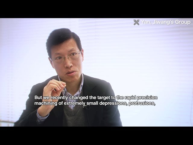
Q "Conventionally, creating a smooth surface is the objective of machining. But we recently change the target to the rapid precision machining of extremely small depressions, protrusions, and surface microstructures, to discover and create new functions for increasing added value of products. That's our main approach.
For example, in electrical discharge machining to fabricate diamond micro-cutting tools, we've confirmed that processing efficiency and accuracy can be improved many times if we incorporate chemical reactions effectively into the electrical discharge machining process. Another example is mechanical machining will inevitably cause a damaged layer in materials. Conventionally, the damaged layer was removed by removing a surface layer from the material by polishing. But we direct a laser beam on the material, which restores the damaged layer back to its original state instantaneously. This is called laser recovery technology. We're proposing new technologies like this."
As well as micro-electrical discharge machining and laser processing technologies, the Yan Laboratory conducts a range of interdisciplinary R&D projects. For example, by forming extremely small depressions, protrusions, and grooves on material surfaces precisely using machining techniques at the micro and nanoscales, the Lab is creating various new surface functions, including water-repellent surfaces, micro-lens arrays for optical control, and micro-channels for protein analysis.
In addition, the lab is now working to develop a new type of lithium-ion battery, using waste silicon powders produced in large amounts during semiconductor manufacturing.
Through such research, the Yan Laboratory intends not only to create new products with higher added value, but also to help society conserve resources and energy.
Q "A feature of our lab is, we combine fundamental research and applied research effectively. We not only do academic research, but also conduct developments for practical applications, to enable our new technologies to be used in industry timely.
In the research of manufacturing technology, I think collaboration between industry and university is extremely important. No matter how hard you have worked to develop a new technology, it is meaningless if it isn't used. This is why we do collaborative research with a range of companies. Through such collaboration, we aim to apply the results of our research to industry as soon as possible."
Creating value, creating knowledge, and creating human resources...
The Yan Laboratory will keep pursuing its R&D, aiming to achieve social contributions through research and education.
The precision of manufacturing technology has advanced from the micrometer to sub-micrometer level, and recently, to the nanometer scale. In the near future, manufacturing techniques are expected to reach the precision level of operating individual atoms.
At Keio University, the Yan Laboratory, in the Department of Mechanical Engineering (Faculty of Science and Technology), is researching ultra-precision manufacturing technologies based on machining and material processing at the nanometer scale, and even at the atomic level.
In high-precision machining and nano processing, the aim is to maximize material functions, and create entirely new functions to materials that transcend their inherent characteristics. The goal is to maximize the added value of important industrial products.
Q "Conventionally, creating a smooth surface is the objective of machining. But we recently change the target to the rapid precision machining of extremely small depressions, protrusions, and surface microstructures, to discover and create new functions for increasing added value of products. That's our main approach.
For example, in electrical discharge machining to fabricate diamond micro-cutting tools, we've confirmed that processing efficiency and accuracy can be improved many times if we incorporate chemical reactions effectively into the electrical discharge machining process. Another example is mechanical machining will inevitably cause a damaged layer in materials. Conventionally, the damaged layer was removed by removing a surface layer from the material by polishing. But we direct a laser beam on the material, which restores the damaged layer back to its original state instantaneously. This is called laser recovery technology. We're proposing new technologies like this."
As well as micro-electrical discharge machining and laser processing technologies, the Yan Laboratory conducts a range of interdisciplinary R&D projects. For example, by forming extremely small depressions, protrusions, and grooves on material surfaces precisely using machining techniques at the micro and nanoscales, the Lab is creating various new surface functions, including water-repellent surfaces, micro-lens arrays for optical control, and micro-channels for protein analysis.
In addition, the lab is now working to develop a new type of lithium-ion battery, using waste silicon powders produced in large amounts during semiconductor manufacturing.
Through such research, the Yan Laboratory intends not only to create new products with higher added value, but also to help society conserve resources and energy.
Q "A feature of our lab is, we combine fundamental research and applied research effectively. We not only do academic research, but also conduct developments for practical applications, to enable our new technologies to be used in industry timely.
In the research of manufacturing technology, I think collaboration between industry and university is extremely important. No matter how hard you have worked to develop a new technology, it is meaningless if it isn't used. This is why we do collaborative research with a range of companies. Through such collaboration, we aim to apply the results of our research to industry as soon as possible."
Creating value, creating knowledge, and creating human resources...
The Yan Laboratory will keep pursuing its R&D, aiming to achieve social contributions through research and education.
- Category
- 教育 - Education
Sign in or sign up to post comments.
Be the first to comment
Up Next
Autoplay
-
02:06

Low-cost Prosthetic Limb Socket Manufacturing Technology #DigInfo
-
39:56
IF Conference 2018 - Blockchain & AI: Opportunities and Challenges
-
01:42
Google 広告活用事例(アプリ マーケティング:FiNC Technologies)
-
04:47
The technologies developed in Kakuda will evolve the space transpotation in future
-
1:29:59
Asia in the Global Economy: Potential Growth & Looming Challenges
-
01:39
UFC Nashville: Anthony Pettis - 'This is Who I am. I Take the Big Challenges'
-
02:52
Micro Electroly Jet Machining Technologies
-
04:25
Creating a concept of value for the next-generation through mechanism research.
-
01:45
Automotive Component 'Net Shape' Manufacturing Technology #DigInfo
-
02:37
Tank Manufacturing Plant Exclusively for Stainless Steel Products
-
02:32
Promoted: SEAT Ateca on tour – a family SUV with added style
-
05:51
Visiting a Japanese Manufacturing Factory 宇部興産機械のデカイ機械を見てきた!
-
1:19:17
Has the Japanese Economy Changed? Challenges & Prospects
-
03:16
Promoted: Nissan X-Trail – the SUV with added versatility
-
30:51
VODCAST | Great value '90s classics | TT meets RAV4
-
01:33
Promoted: Ssangyong Tivoli – great value to buy and run
-
12:48
Ready to Face New Challenges
-
13:10
3 CHALLENGES IN 1 - Blindfolded, Wrong Hand, 3 Markers
-
00:49
"Challenges Motivate Me" #becomingafighter
-
05:11
Advanced nanometer-scale manufacturing technologies #DigInfo
-
03:06
Jack Della Maddalena: 'All That Added Pressure Just Makes a Victory Feel That Much Better' | UFC 284
-
08:58
2019 Porsche 718 Cayman T driven | Is this the best value Cayman? | Autocar